ECE1388 Final Project
Binary Serial Hybrid Digital to Analog Converter
Ritu Raj Singh
995140752
The existing charge scaling digital to analog converters (DAC) architectures namely the Binary Weighted DAC (BWDAC) and the Serial DAC (SDAC) are located on the extreme corners of an Area-Speed plot. BWDACs are fast (1 clock cycle conversion), accurate but occupy a lot of area (2NC, where N is the resolution of the DAC). On the other hand SDACs occupy small area, independent of the DAC resolution but are slow (N clock cycle conversion) and suffer from charge injection errors. The proposed DAC architecture trades area with speed thereby increasing the flexibility of implementation based on the area, speed specifications. That is, capacitor resources of a low resolution DAC are used to achieve a higher resolution.
1. Proposed Design
Figure 1 self explains the working of a 6 bit resolution DAC implemented using a modified form of a 2 bit Binary Weighted DAC and takes 3 clock cycles for conversion. Each clock cycle the voltage on the terminating capacitor gets divided by 4 to achieve the desired binary ratio for the corresponding input bits of the binary word.
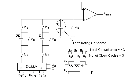
Figure 1. A 6 bit Binary Serial Hybrid DAC
using 2 bit BWDAC resource
Voltage of the terminating capacitor after
1st clock cycle:
![]()
2nd clock cycle:
![]()
3rd clock cycle and final voltage:

2. Design Specifications
DAC specifications:
|
DAC architecture |
6 bit BWDAC-2 clock cycle |
|
DAC resolution |
12 |
|
Reference voltage |
1.2 Volt |
|
Speed |
As high as possible |
|
Technology |
0.35um TSMC |
Opamp specifications:
|
Gain |
80 dB |
|
Phase margin |
80 degrees |
|
Slew rate |
40V/ us |
|
Bandwidth |
1 MHz |
3. System Overview
Figure 2, shows the block diagram of the design. The capacitor array along with the opamp is inside the Hybrid DAC block. The input digital word is fed to the Switch Array block which acts as a multiplexer and also a driver for the capacitor array in the Hybrid DAC block. The clock generator generates clocks with different phases for use in the Hybrid DAC and the Switch Array block.
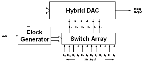
Figure 2. Block Diagram of the DAC
Figure 3, shows the waveform view of the input and the output.

Figure 3. Clock Waveforms for the DAC
3.1 Hybrid DAC block
Figure 4, shows the schematic of the DAC block used. A 12 bit resolution was targeted with the passive capacitor array network. A 6 bit-2 clock cycle DAC architecture, was chosen to implement the same. From CMOP35 mismatch model [1] and thermal noise considerations [2] the unit capacitor size was chosen to be 500fF. Since, in the given specification, the linearity of the DAC is given more weightage, therefore the switches have been implemented using only nMOS transistors. Use of transmission gates introduces harmonics and an imbalanced charge injection cancellation.
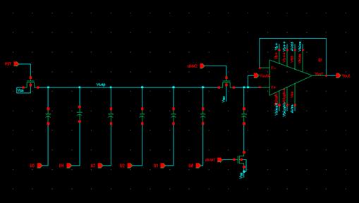
Figure 4. Clock Waveforms for the DAC
The voltage of the terminating capacitor is the DAC voltage and care should be taken not to introduce errors while connecting-disconnecting the terminal capacitor from the rest of the capacitor network. Bottom sampling technique has therefore been used use to minimize such errors. When disconnecting the terminating capacitor, the bottom transistor (connected to clkM1) is switched off a little earlier than the top transistor (connected to clkM2). This forces the input dependent charge injection of the clkM2 transistor towards the left (not on the terminating capacitor). The charge injection of the clkM1 transistor appears as a constant offset on the DAC output. The transistor sizes have been kept small so that their parasitic capacitance is negligible as compared to the capacitor array.
The reset transistor (connected to RST) resets the capacitor array. Its size requirement has been relaxed by parallely applying an input 0 at the capacitor ends.
3.2 Switch Array
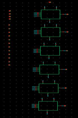
Figure 5, shows the schematic of the Switch Array used. The block is essentially a multiplexer with different sizing inorder to ensure similar charging times for the binary weighted capacitors.
 `` `
`` `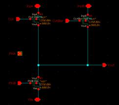
Figure 5. Switch Array Schematic Figure 6. Unit cell schematic
(Switch Array)
Figure 6, shows the schematic for a single bit. Previously, logical effort was tried to ensure similar rise times, however because of the large delay of the gates, speed more than 10MHz could not be achieved (between the output of the Switch Array and the clkM1 and clkM2). Moreover, the high output of the gates varied from 1.199V to 1.2V, which changed the DAC reference voltage. Figure 7 shows the schematic for the previously implemented logical effort gate array.
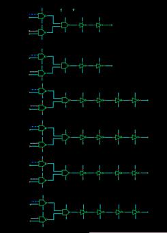
Figure 7. Previous implementation using Gate arrays
3.3 Clock Generator
block
Figure 8, shows the schematic of the Clock Generator used. In order to ensure proper timing of the various clocks to the DAC and the Switch Array, with balanced time delay between the various phases and low skews, the gate sizes have been tuned. The passive capacitor network is able to achieve a 12 bit performance upto 40MHz.
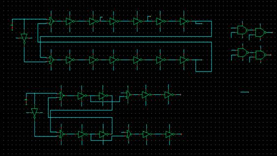
Figure 8. Clock generator schematic
3.4 Operational amplifier
Figure 8, shows the schematic for the operational amplifier used. Since the input to the opamp could be close to 0, a pmos input pair folded cascade topology was used for the opamp. An additional common source stage was added to achieve the high gain of 80dB. Previously, it was planned to have the operational amplifier in a feedback mode, but because of the high capacitive load of 32pF and the slew rate requirements, the opamp design was unreasonable and hence the opamp was then just kept as a voltage buffer.
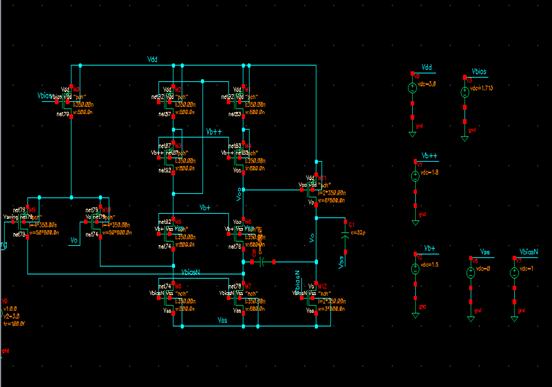
Figure 9. Opamp schematic
4. Simulation results
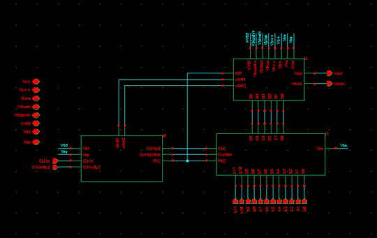
Figure 10. Top level Schematic
Figure 10 shows the top level schematic used for simulation. Figure 11 shows the simulation results for the DAC without the opamp at 1KHz. Figure 12 shows the simulation results for the DAC with the opamp at 20KHz. Figure 13 shows the DNL plot of the DAC without the opamp. Due to lack of time, the DNL plot with the operational amplifier could not be done. But from the simulation results, the error in voltage with the opamp was around 100uV, which suggests an effective resolution of 10 bits. Figure 14, shows the operational amplifier gain and phase margin plot.
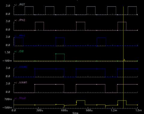
Figure 11. Simulation results without the opamp
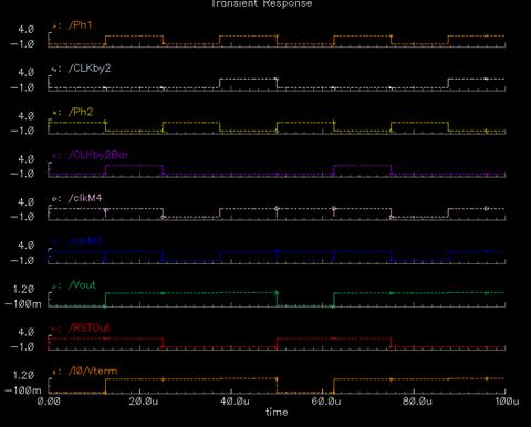
Figure 12. Simulation results with the opamp
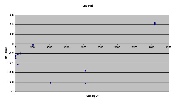
Figure 13. DNL plot for the DAC without the opamp
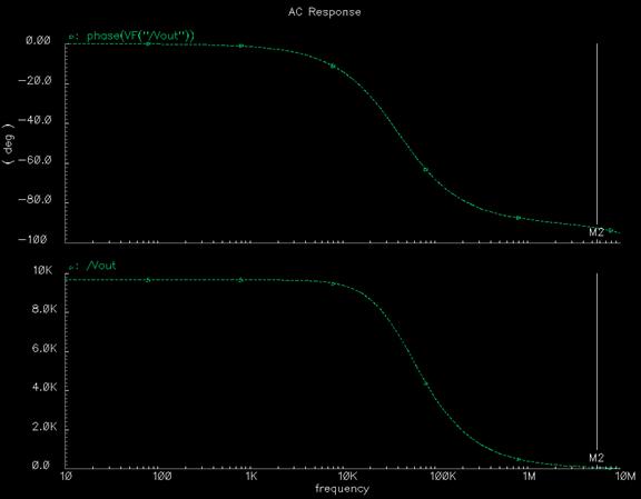
Figure 14. Opamp simulation for gain and phase margin
5. Layout:
The determining factor in the size of the layout is the length of the capacitor array. Therefore the layout of the other blocks that is the switch array and the clock generator have been done to align with the length of the capacitor array.
5.1 Capacitor Array
The capacitor layout for a digital to analog converter needs to be done with care inorder to minimize mismatches between the capacitor ratio. Any such mismatch will reflect in the linearity of the DAC. Following techniques have been used for the layout:
a) Common centroid technique : The chip is symmetric along the X and the Y axis
b) Dummy capacitors: Dummy capacitors have been places along the capacitor array to reduce the electrostatic interference from the surrounding circuitry.
c) Minimum aspect ratio
d) Similar unit blocks
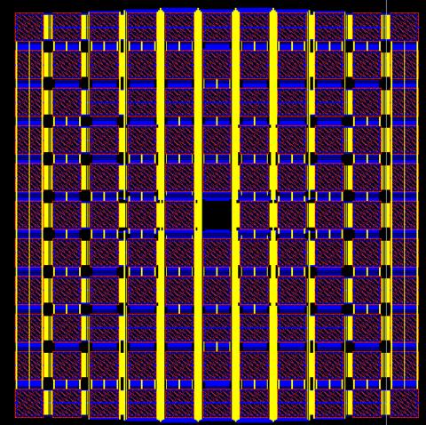
Figure 15. Capacitor Array layout
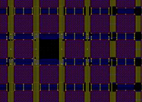
Figure 15. Capacitor Array layout (magnified)
5.2 Switch Array
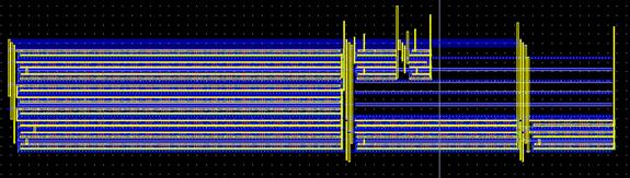
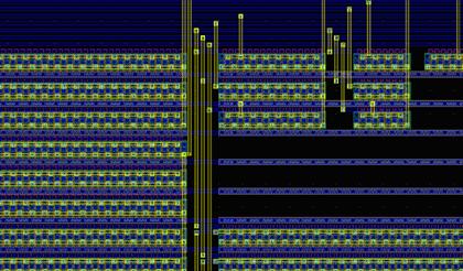
Figure 16. Switch Array layout
5.3 Clock Generator
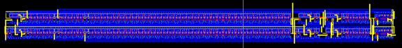
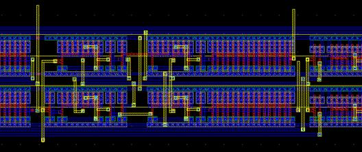
Figure 17. Clock Generator layout
5.4 Operational
Amplifier
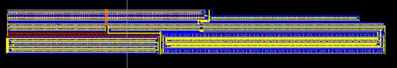
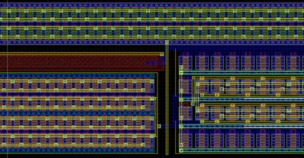
Figure 18. Operational amplifier layout
5.5 Full Chip Layout

Figure 19. Floor assignment
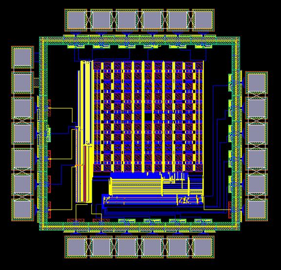
Figure 20. Full Chip layout
Future Work:
Due to lack of time, the operational amplifier in feedback mode for parasitic cancellation technique could not be tested properly. Also, it will be worthwhile to plot a frequency spectrum of the DAC to see the SNDR performance.
References
1. G. Nikandish, B. Sedighi, M. Sharif Bakhtiar, “INL prediction method in pipeline ADCs”, IEEE Asia-Pacific Conference on Circuits and Systems, 2006.
2. B. Razavi, Design of Analog
CMOS Integrated Circuits.